

Moore's Law was kind of like the golden rule for computer systems. Developed by Intel cofounder Gordon Moore, the rule has been the centrepiece and fundamental principle behind the ever-improving computer systems we have today. It basically spelt out the future in that computers will get better performance year after year (doubling in performance, roughly).
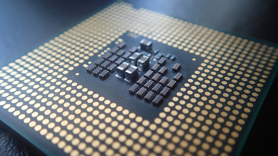
It did this by not increasing the package size of the CPUs but by reducing the feature size. Take my EliteBook for example. It has a Ryzen 6850U processor, built with a 7-nanometer process. This 7-nanometer process is called fabrication, and it roughly means that the size of each transistor within a package (a CPU die) is around that size. The smaller and smaller the feature size the more and more likely it is for something to fail or go wrong during production, making it more and more difficult to manufacture CPUs as the feature sizes get smaller. Not only that, it has always been said that we will be unable to get the feature size smaller than the size of an atom (which is approximately 0.1 nanometers in size). The theoretical boundary for the smallest feature size that we can manufacture is approximately 0.5 nanometers - that's not that far away from where we are at 4 nanometers in 2023.
Over the last few years, manufacturers have been trying to squeeze every bit of performance increase out of the latest chips. Apple has been increasing the physical size of the processors by adding several chips together (think of the M1 Pro and Max which are simply M1 chips stuck together with a little bit of magic). This makes the processor very large and unsuitable for smaller devices. AMD, on the other hand, has moved to a design where wastage is less frequent thus increasing the yield of good processors and in turn allowing them to cram more performance into their dies.
To combat such an issue, the manufacturers of some CPUs moved to a chiplet design. This chiplet design is basically where several components such as the memory controller, IO controllers such as USB and so on compared with the original monolithic architecture used in the past. The first time I experienced a chiplet-based CPU was the Intel Core 2 Quad, where it was literally two Core 2 Duo dies on one chip. The issue is that it takes more space than building a chip using a monolithic architecture where the entire processor resides within one die. There are also other complications such as communication internally between these dies, but they can be easily overcome once it's been done with one chip, as the designs can continue to be used in other chips. There are also power consumption concerns when two CPU dies are put on the same chip, but with chiplets for IO and memory, this actually reduces the distance between the CPU and the chip, thus actually reducing power consumption and increasing performance. Chiplet design also keeps costs down as it reduces binning a good processor when a section of it fails. For example, if all IO was built into the actual CPU die (as is the case in a monolithic architecture) and only one part of the IO section failed, the whole processing unit would be binned. With a chiplet design, if there is a failure in the IO section, it happens only in that chiplet - a much less costly fix as all it would require is a replacement IO die.
Another way manufacturers are continuing to squeeze performance out of these chips is by embedding algorithms in them. This has always been a feature of CPUs since the Pentium MMX which brought several instruction sets to improve the multimedia capabilities of computers back then. It basically means that instead of a programmer writing an algorithm say to do the vector encoding using something like AVX-512, the CPU does not need the user to write the program. The program is actually an instruction built into the CPU and therefore it runs much faster. This is called hardware encoding. You'll see that Apple has done a lot of this in their M1 and M2 chips over the years to give them an even better performance result than the Intel CPUs they replaced. By doing this, Apple has managed to improve the effectiveness of its software through the use of hardware. This is actually something that could become a problem, however, and it might damage the cross-compatibility of software that can run on any operating system and any platform. I say this because if a piece of software is developed to use AVX-512 it's very likely that it will work on a system without AVX-512 instructions. But with an instruction being built-in such as one which utilises libraries specific to a GPU or CPU feature, cross-compatibility may not be possible without writing massive amounts of additional code (for example DirectX or Metal on macOS both cause issues when porting).
I have always believed since I was a teen that the second method is indeed the way forward, but it really would only work in a single CPU/GPU architecture world, a bit like if everyone was using x86. That's never going to happen, but perhaps if we had a library (Vulcan) that could abstract over those underlying APIs or hardware and make things simpler for developers, then maybe this is actually the best option.